
VNA Prototyping Board
Some years ago, SDR-Kits used to sell a small prototyping PCB perfect for experimenting with a Vector Network Analyzer. After many experiments, the female pin headers on my prototyping board wore out. Since SDR-Kits no longer sells it, I designed my version of this PCB. The KiCad sources of the VNA prototyping/test board are available on my Github profile.
Design considerations
I designed the PCB with KiCad version 7. Most likely, you have to change the footprint of the female SMA connectors on the PCB, since I used non-standard ones I had available at that moment. I designed the traces as microstrip lines, matching 50 Ohm. This resulting trace width is 1.85mm using 1,0mm PCB thickness and an Epsilon r = 4.5 of the FR4 material. I get accurate results up to a few hundred Megahertz. The pin sockets have a 2.54mm spacing. I use Nylon M3 screws & nuts as feet.
You can create a calibration kit with male pin headers and a 1% 50Ohm SMD resistor.
License
I published the Design under the Creative Commons Attribution-ShareAlike 4.0 International.
More pictures
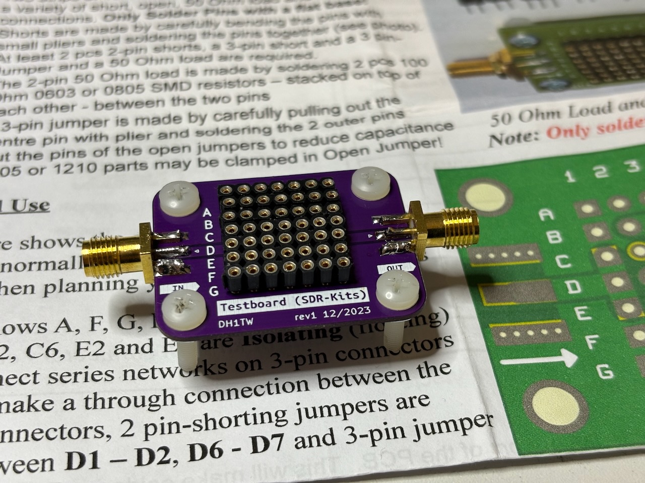
The VNA Testboard
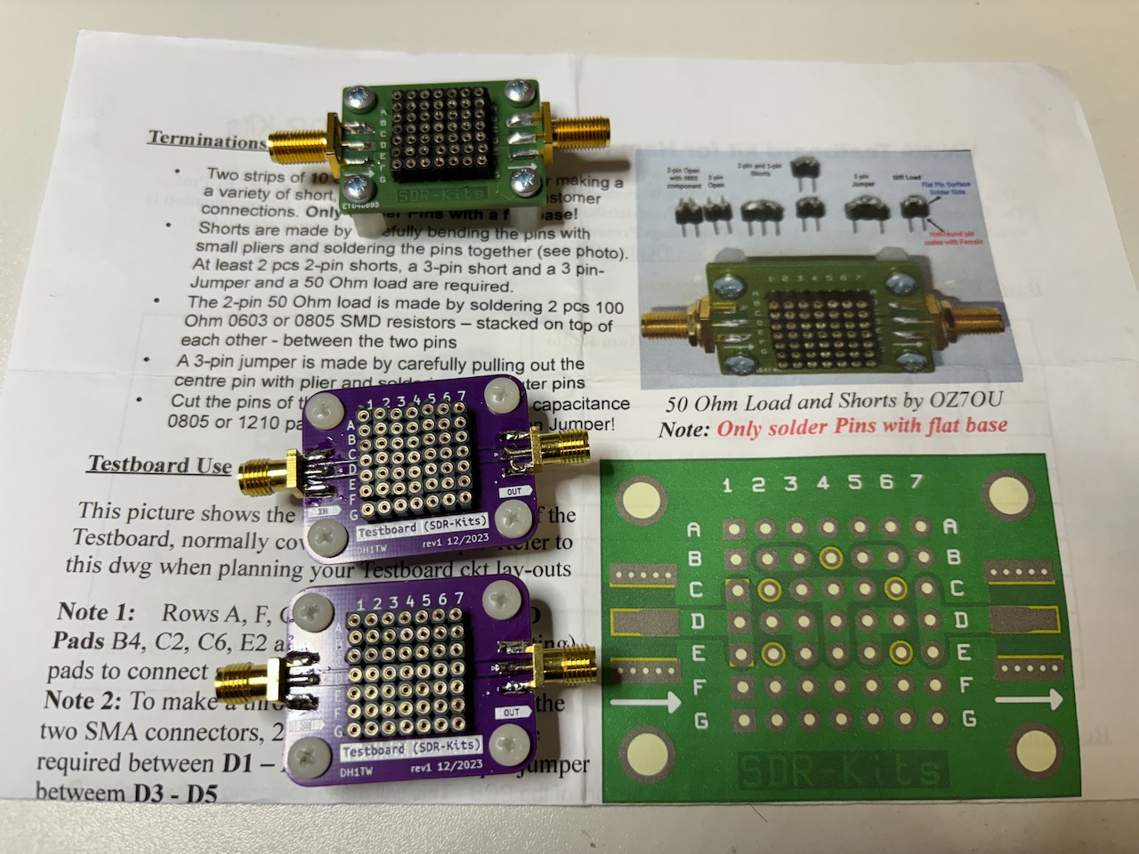
The VNA Testboard with the original one from SDR-Kits
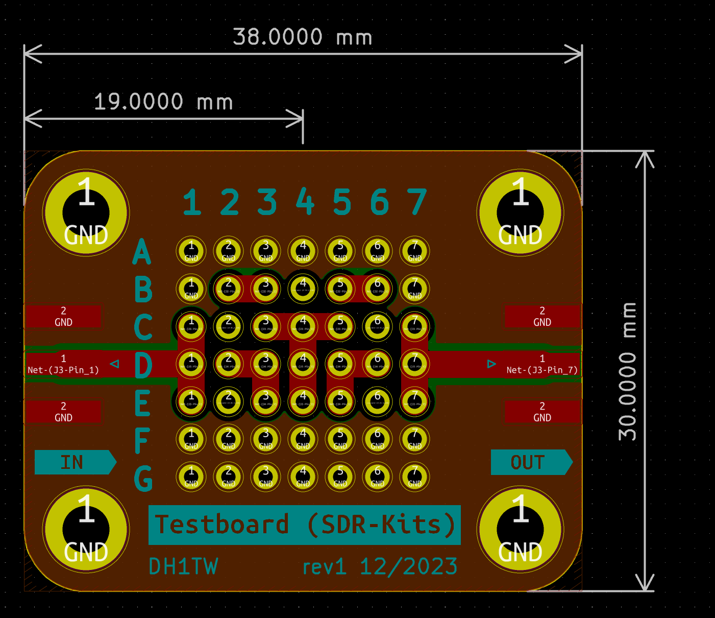
The PCB Layout of the VNA testboard
